
EV On-Board Charger Power Solution with Infineon OptiMOS MOSFET
EV ChargingA high-efficiency EV on-board charger (OBC) solution using Infineon OptiMOS MOSFET devices sourced from BeiLuo. This solution covers totem-pole PFC, phase-shifted full-bridge DC-DC conversion, synchronous rectification, thermal design, and EMI filtering for 3.3 kW to 11 kW AC charging applications.
Key Advantages
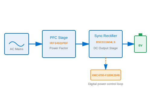
- Infineon IRFS4321PBF OptiMOS MOSFET achieves 3.5 milliohm RDS(on) max in a D2PAK package, minimizing PFC conduction losses at 30 A continuous input current
- BSC011N04LS provides 1.1 milliohm RDS(on) for synchronous rectification on the battery side, raising overall OBC efficiency above 94 percent
- Totem-pole PFC topology with Infineon MOSFETs achieves near-unity power factor and less than 5 percent THD, meeting IEC 61000-3-2 Class A limits
- BeiLuo stocks both MOSFET types for immediate shipment, supporting rapid OBC prototyping and production ramp schedules
Overview of EV On-Board Charger Architecture
The on-board charger (OBC) is one of the most technically demanding subsystems in an electric vehicle. It must accept AC mains input across a wide voltage range (85 to 265 VAC), correct the power factor to near unity, galvanically isolate the grid from the high-voltage battery pack, and regulate output voltage and current over a battery state-of-charge range from 10 to 100 percent -- all while achieving conversion efficiency above 93 percent in a package small enough to fit within the vehicle chassis. Infineon's OptiMOS MOSFET family, specifically the IRFS4321PBF and BSC011N04LS, provides the low on-resistance and fast switching characteristics needed to meet these demanding targets. BeiLuo stocks both parts and supports customer OBC designs from first prototype through volume production.
Totem-Pole PFC Front End
The dominant OBC front-end topology in modern designs is the bridgeless totem-pole power factor correction (PFC) converter. Unlike conventional boost PFC circuits that use a diode bridge rectifier followed by a boost inductor and switch, the totem-pole PFC replaces the rectifier bridge with two additional MOSFETs. This eliminates the rectifier diode forward-voltage drop (typically 0.7 V per diode, or 1.4 V for two series diodes) from the conduction path, reducing front-end losses by 1.5 to 2 percentage points at 230 VAC input.
The IRFS4321PBF is well-suited to the totem-pole PFC switching position. Its 150 V VDSS rating provides adequate margin above the rectified 230 VAC peak (approximately 325 V). The 3.5 milliohm RDS(on) at 25 degrees C (rising to approximately 5.5 milliohm at 100 degrees C) gives a conduction loss of less than 5 W per device at 30 A continuous input current in a 7.2 kW OBC. The D2PAK package mounts directly to the PCB with a thermal pad exposed on the bottom, enabling conduction-cooled designs where the PCB laminate itself serves as an intermediate thermal spreader to the chassis.
Phase-Shifted Full-Bridge DC-DC Converter
After the PFC stage stabilizes the DC bus at 400 V, an isolated DC-DC converter steps down and regulates the output voltage to match the battery pack charging profile (typically 250 to 450 V at currents from 1 to 25 A for a 7.2 kW stage). The phase-shifted full-bridge (PSFB) topology is widely adopted because it achieves zero-voltage switching (ZVS) for the four primary-side MOSFETs under most load conditions, dramatically reducing switching losses. The IRFS4321PBF again serves as the primary-side transistor in this topology, exploiting its 150 V rating and the availability of its body diode for ZVS transitions. The transformer turns ratio is designed so that ZVS range extends from 20 percent to full load, with a small auxiliary inductor added in series with the primary winding to widen the ZVS window at light loads.
Synchronous Rectification with BSC011N04LS
On the secondary side of the isolation transformer, synchronous rectifiers replace conventional Schottky diodes to reduce conduction losses. The BSC011N04LS is a 40 V N-channel OptiMOS MOSFET in a SuperSO8-5 package with an industry-leading RDS(on) of 1.1 milliohm at 10 V gate drive. At a secondary peak current of 40 A in a 7.2 kW converter, the conduction loss per synchronous rectifier device is less than 1.8 W -- less than half the loss of a comparable Schottky diode at the same current. Four BSC011N04LS devices in a center-tap rectifier configuration handle the full output power. Their compact SuperSO8 footprint with exposed drain pad on the underside allows direct mounting to a PCB copper pour that spreads heat to the chassis via thermal vias.
Gate Drive and Dead-Time Requirements
Proper dead-time management between complementary MOSFET pairs prevents shoot-through current while ensuring body diode conduction intervals are short enough to avoid excessive reverse-recovery losses. For the IRFS4321PBF in the totem-pole PFC and PSFB primary side, a dead time of 100 to 200 nanoseconds at 100 kHz switching frequency is appropriate. Gate drive voltage of +10 V for the IRFS4321PBF minimizes RDS(on) while avoiding excessive gate charge losses. For the BSC011N04LS synchronous rectifiers, self-driven gate drive using the transformer secondary voltage simplifies the control circuit and ensures that synchronous rectifier turn-on and turn-off tracks primary switching events without controller intervention.
EMI Filtering and Thermal Design
A two-stage differential-mode EMI filter at the AC input (common-mode choke plus X-capacitors) suppresses conducted emissions below the CISPR 25 Class 5 limit applicable to automotive OBCs. The dominant noise sources are the totem-pole PFC switching transitions at 65 to 100 kHz. Careful PCB layout minimizing the high dV/dt loop area between the PFC switching node, the DC bus capacitor, and the MOSFET drain pin is the most effective EMI mitigation technique. Adding a small RC snubber of 10 ohms and 1 nF across each PFC MOSFET drain-source limits peak ringing voltage to less than 120 percent of steady-state drain voltage.
The overall OBC thermal stack uses a die-cast aluminum housing that also functions as a heat sink. The IRFS4321PBF D2PAK devices mount to the housing via thermally conductive silicone pads, while the BSC011N04LS SuperSO8 devices conduct heat through PCB copper pours and thermal vias to the housing floor. This approach achieves a housing-to-ambient thermal resistance below 0.3 K/W with forced air, enabling a 7.2 kW OBC to operate at 65 degrees C ambient with all semiconductor junction temperatures below 125 degrees C.
Application Scenarios and BeiLuo Supply
OBC designs using Infineon OptiMOS MOSFETs from BeiLuo cover power levels from 1.5 kW single-phase systems in two-wheel EVs to 11 kW three-phase units in commercial fleet vehicles. Battery electric cars, plug-in hybrids, electric buses, and stationary energy storage systems all benefit from the efficiency and power density that Infineon OptiMOS technology enables. BeiLuo provides volume stock of IRFS4321PBF and BSC011N04LS, along with FAE schematic review, gate timing optimization, and thermal simulation support, helping customers meet SAE J1772 and IEC 62955 OBC standards efficiently.
Bill of Materials
| Part No. | Description | Qty |
|---|---|---|
| IRFS4321PBF | 150 V N-channel OptiMOS MOSFET in D2PAK -- PFC stage switching device and primary-side bridge transistor | 4 |
| BSC011N04LS | 40 V N-channel OptiMOS MOSFET in SuperSO8 -- synchronous rectifier on battery-side secondary winding | 4 |
| XMC4700-F100K2048 | 144 MHz ARM Cortex-M4F MCU with CCU8 PWM unit -- PFC and phase-shifted full-bridge control loop | 1 |
Ready to Build This Solution?
Contact BeiLuo for component sourcing, FAE support, and reference designs.
Get BOM Quote